Overview of the HCF4050B Hex Buffer/Converter
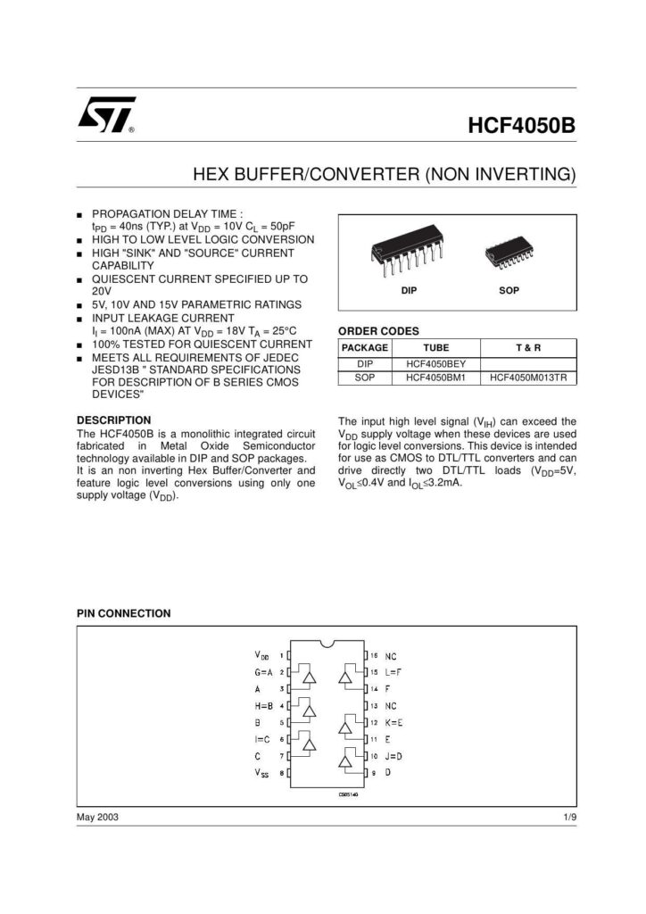
The HCF4050B is a high-performance Hex Buffer/Converter that operates non-invertingly and is fabricated using Metal Oxide Semiconductor technology. Designed to handle high “sink” and “source” current capabilities, this integrated circuit is suitable for high to low-level logic conversions and is available in DIP (Dual In-line Package) and SOP (Small Outline Package) variants.
Key Features
The HCF4050B is characterized by a typical propagation delay time (tpD) of 40ns at a supply voltage (VDD) of 10V and a capacitive load (CL) of 50pF. It stands out for its performance with high quiescent current specifications provided at various supply voltages of 5V, 10V, and 15V and remains within the JESD13B standard specifications for B series CMOS devices. Another critical feature includes its ability to maintain an input leakage current (Ip) of a maximum of 100nA at an 18V VDD and a 25°C ambient temperature.
Ordering Codes and Packaging
Datasheet provides ordering information, indicating the device’s availability in tube packaging for DIP configuration (HCF4050BEY) and Tape & Reel for SOP design (HCF4050M013TR).
Functional Description
As a CMOS to DTL/TTL converter, the HCF4050B has the capability to directly drive two DTL/TTL loads and allows for logic level conversion even when input signals exceed the supply voltage. This is particularly significant for mixed voltage system designs.
Pin Configuration and Function
The integrated circuit includes multiple data input pins (A, B, C, D, E) and data output pins (G, H, I, J, K). Additionally, it incorporates pins for positive supply voltage (VDD), negative supply voltage (VSS), and not connected (NC) terminals for added flexibility in circuit integration.
Electrical Characteristics
Absolute Maximum Ratings detail the limits of the HCF4050B’s operation, ensuring users avoid conditions that may damage the device. The supply voltage ranges from -0.5V to +22V, with an input voltage range of -0.5V to +18V. For safe operation, the recommended conditions suggest a supply voltage of 3V to 20V and operating temperatures ranging from -55°C to +125°C.
Device Protection and Reliability
The device includes built-in ESD protection and a truth table that defines its logical behavior. It emphasizes 100% testing for quiescent current to ensure device reliability in various applications.
References:
Chat: Powered By VoiceSphere
Pricing & Distributors: https://www.datasheets360.com/part/detail/hcf4050m013tr/-3921324308959589787/

