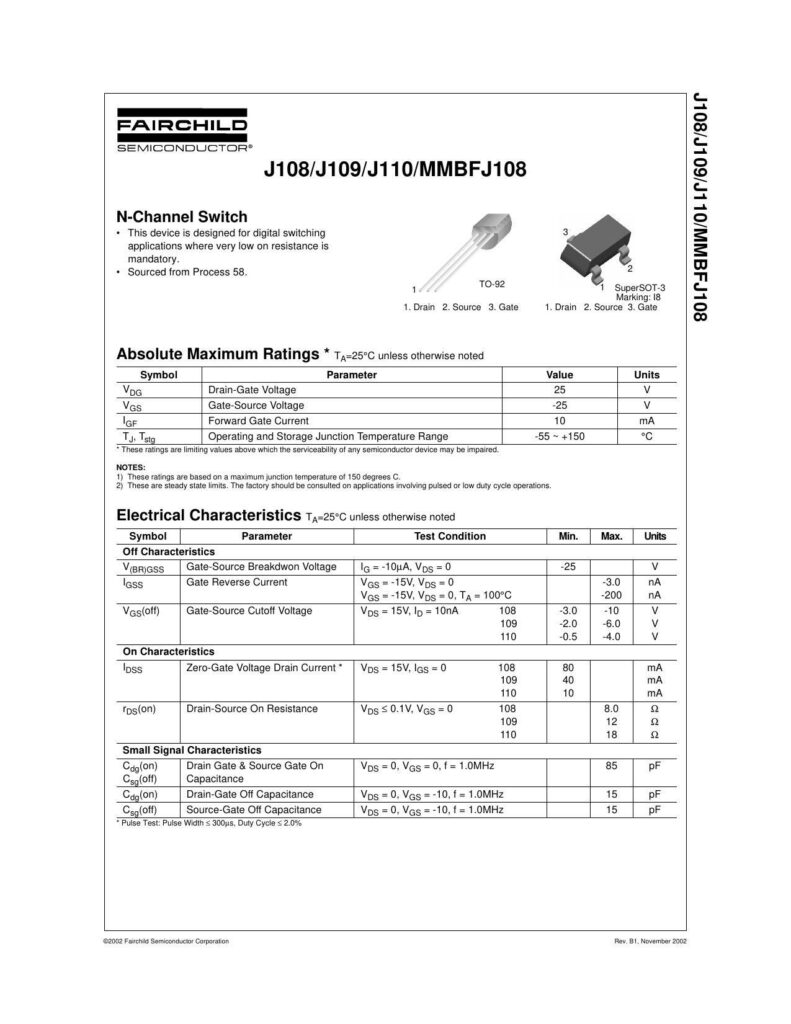
N-Channel Switch
This device is designed for digital switching applications where very low on resistance is required.
Absolute Maximum Ratings
The device has a maximum drain-gate voltage of 25V, gate-source voltage of ±25V, and forward gate current of 10mA.
Electrical Characteristics
The device has a gate-source breakdown voltage of 25V, gate-source cutoff voltage of 3.0V, and drain-source on resistance of 6.0Ω.
Thermal Characteristics
The device has a total device dissipation of 1.6W, derate above 25°C, and thermal resistance, junction to case of 125°C/W.
The datasheet also provides typical characteristics, including graphs for parameter interactions, drain-source voltage, gate-source voltage, and noise voltage vs frequency.
Manual:
Chat: Powered By VoiceSphere
Pricing & Distributors: https://www.datasheets360.com/part/detail/j108d27z/-4413644901352239883/