Overview
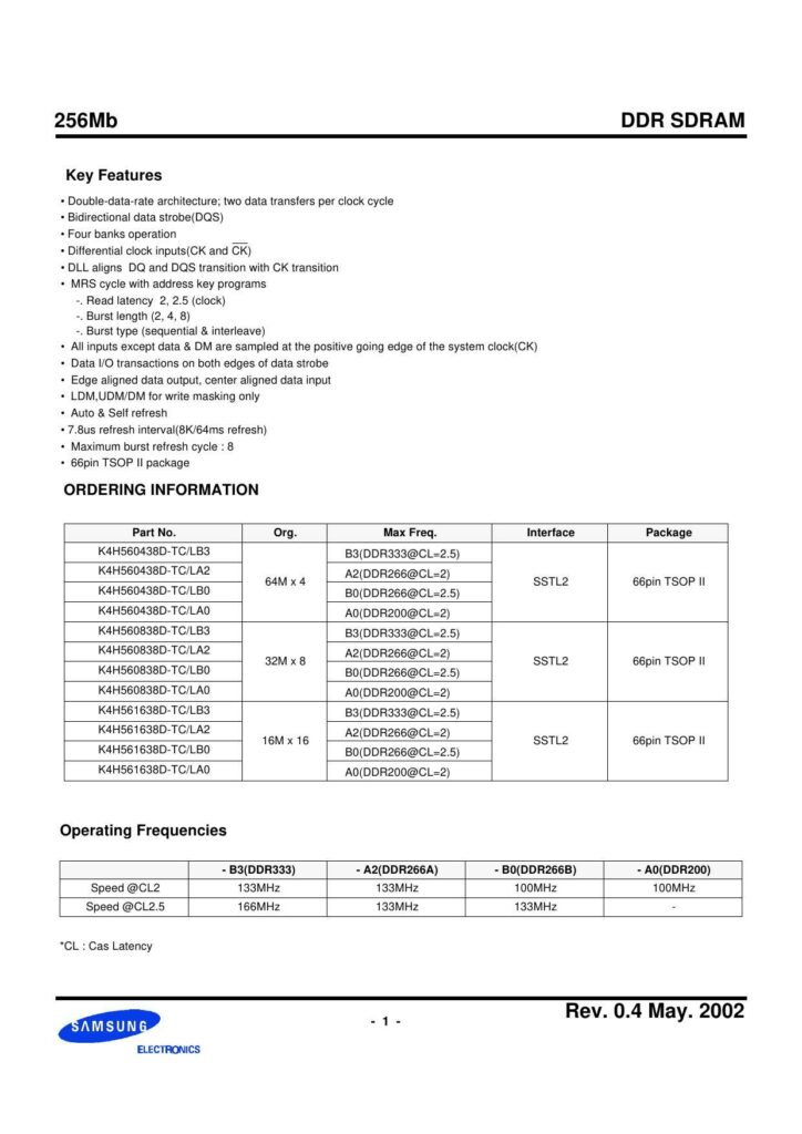
This DDR SDRAM features a double-data-rate architecture, bidirectional data strobe (DQS), and four banks operation.
Key Features
It has a differential clock input (CK and CK), DLL aligns DQ and DQS transition with CK transition, and MRS cycle with address key programs.
Read latency is 2, 2.5 (clock), and burst length is 2, 4, 8 with sequential and interleave burst types.
All inputs except data and DM are sampled at the positive going edge of the system clock (CK).
Data I/O transactions occur on both edges of the data strobe, with edge-aligned data output and center-aligned data input.
It also features LDM, UDM, and DM for write masking only, auto and self-refresh, and a 7.8us refresh interval (8K/64ms refresh).
The maximum burst refresh cycle is 66, and it comes in a 66-pin TSOP II package.
Manual:
Chat: Powered By VoiceSphere
Pricing & Distributors: https://www.datasheets360.com/part/detail/k4h561638d-tcb3/5192240600968867060/

