Overview of the IBM High-Performance SRAM
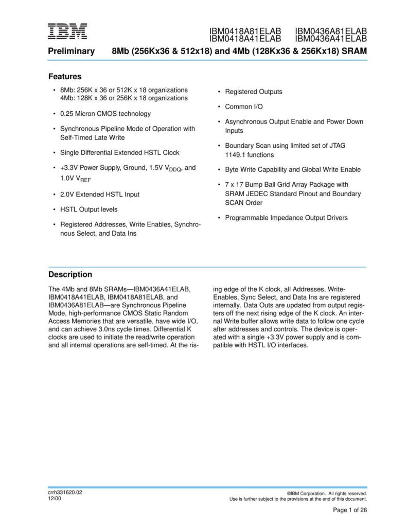
This preliminary datasheet describes the features and operational details of IBM’s high-performance synchronous pipeline static random-access memories (SRAM) with capacities of 4Mb and 8Mb. The two SRAM variants are offered in different configurations: the 8Mb is available in 256K x 36 or 512K x 18 organizations, and the 4Mb is offered in 128K x 36 or 256K x 18 organizations. These devices have been engineered utilizing advanced 0.25 Micron CMOS technology, emphasizing their efficiency and high-speed functionality.
Key Features
Registered Outputs and Common I/O: Streamlining the output process and enabling easier integration with existing systems.
Asynchronous Output Enable and Power Down Inputs: Provide additional control capabilities and power management features for improved energy conservation.
Synchronous Pipeline Mode: Ensures fast and reliable operation, further improved by self-timed late write functionality.
Boundary Scan: Limited set of JTAG 1149.1 functions for easier testing and debugging.
Power Supply Compatibility: The devices are powered with a single +3.3V source and accommodate 2.0V HSTL inputs with HSTL output levels.
Byte Write Capability and Global Write Enable: Offer flexibility in programming and increased efficiency in the write process.
Programmable Impedance Output Drivers: Flexibility in adapting the output characteristics to different system requirements.
Description and Operation
The models IBMO436A41ELAB, IBMO418A41ELAB, IBMO418ABIELAB, and IBMO436A81ELAB are designed for high-speed operations reaching cycle times up to 3.0ns. Central to their operation is the use of differential K clocks that initiate read/write cycles and ensure all internal activities are precisely timed. Critical information including addresses, write enables, synchronous select, and data inputs are captured internally on the rising edge of the K clock. Outputs are then updated on the subsequent rising edge.
The integration of an internal write buffer allows for write data to be sequenced one cycle after addresses and controls, enhancing the overall efficiency of the device. These SRAM models are engineered for holistic compatibility with HSTL I/O interfaces, making them suitable for a broad range of technology applications needing high-speed and reliable memory solutions.
Package and Pin configurations
Presented are two top views of the Ball Grid Array (BGA) packaging for both x36 and x18 configurations, exhibiting the placement of power, ground, data I/O, and clock mode pins. Specifically, the diagrams indicate how M1 and M2 clock mode pins should be connected, which is crucial for the accurate functioning of the memory devices.
References:
Chat: Powered By VoiceSphere
Pricing & Distributors: https://www.datasheets360.com/part/detail/ibm0418a81elab-3/-4051163126129598806/

