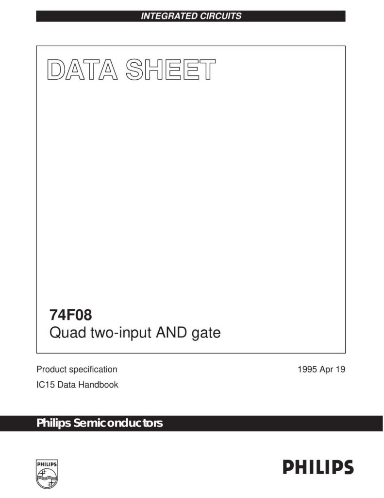
Overview of Philips 74F08 Quad Two-Input AND Gate
The 74F08 is an integrated circuit designed by Philips Semiconductors as a quad two-input AND gate. This product specification is included in the IC15 Data Handbook, and the datasheet’s initial issue is dated 1995 Apr 19. The 74F08 facilitates four individual 2-input AND gates in a single chip, and this device is offered in various temperature ranges, making it suitable for both commercial and industrial applications.
Key Specifications
Temperature Ranges:
The device operates in two designated temperature ranges:
- Commercial range: 0°C to +70°C with a supply voltage (Vcc) of 5.0V ±10%
- Industrial range: -40°C to +85°C with a similar Vcc margin
Supply Current and Propagation Delay:
The 74F08 features a typical supply current (total) of 7.1mA and a typical propagation delay of 4.1ns, striking a balance between energy efficiency and performance speed.
Package Options and Ordering Information
Available package types include a 14-pin plastic DIP (Dual In-line Package) and a 14-pin plastic SO (Small Outline) with respective ordering codes NZ4FOBN and N74FO8D for the commercial range, and I74FO8N and I74FO8D for the industrial range. The package drawing numbers are SOT27-1 and SOT108-1.
Pin Configuration and Logic Details
The data inputs (Dna, Dnb) are specified with a load value high/low of 20µA/0.6mA and 1.0mA/0mA respectively, whereas the data output (Qn) has a load of 50/33. The defined FAST unit load gives current specifications for the high and low states of inputs and outputs, which is critical for understanding the interfacing capabilities and limitations.
Functional Connection and Usage
The logic diagram and function table provided offer users a clear illustration of the chip’s internal connections, which represent a straightforward implementation of the AND logic, where each gate’s output is high only when both its inputs are high. The logic symbols comply with IEEE/IEC standards for ease of recognition in global electronics designs. The Vcc and GND pins are designated as pin 14 and pin 7 respectively, observing standard practice for IC power connections.
Final Remarks
For engineers and electronics designers seeking a reliable and efficient quad two-input AND logic gate for their digital circuits, the 74F08 is emphasized as a relevant solution. The datasheet provides all necessary technical details for proper implementation and ensures compliance with traditional logic design standards.
References:
Chat: Powered By VoiceSphere
Pricing & Distributors: https://www.datasheets360.com/part/detail/n74f08n/4250344706150650305/

