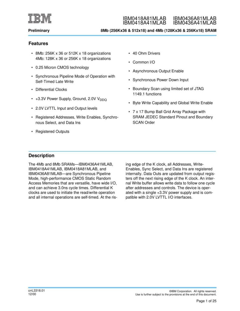
The datasheet details the specifications and features of the IBM Synchronous Pipeline Mode Static Random Access Memories (SRAMs) with storage capacities of 8Mb and 4Mb. These high-performance memory chips are available in two organizational forms: for the 8Mb version, a 256K x 36 or 512K x 18 setup, and for the 4Mb version, a 128K x 36 or 256K x 18 setup.
Key Features
The SRAMs are built on a 0.25 Micron CMOS technology and are equipped with 40 Ohm drivers for efficient operation. Their functionality includes Common I/O capabilities, Asynchronous Output Enable, and Synchronous Pipeline Mode operation with a Self-Timed Late Write feature that improves write efficiency. They offer Synchronous Power Down Input, facilitating low-power states, and Differential Clock inputs for accurate signaling.
Additionally, these memory modules support a Boundary Scan feature compatible with a select set of JTAG 1149.1 functions, enabling easier testing and verification of the chip’s integrated circuits. Both variations are designed to work with a +3.3V power supply and ground, while also supporting 2.0V VDDQ for different power configurations. They further support Byte Write Capability and Global Write Enable, allowing for flexible data manipulation, and are compatible with 2.0V LVTTL Input and Output levels.
Physical Design
The physical package of these SRAMs is a 7 x 17 Bump Ball Grid Array (BGA), adhering to the JEDEC Standard Pinout and Boundary Scan Order. This compact and grid-based design simplifies PCB layout and enhances connection reliability.
Operation and Performance
The SRAMs operate in a Synchronous Pipeline Mode which delivers a high-performance output with the ability to achieve cycle times as fast as 3.Ons. They use Differential K clocks for initiating read/write operations. Internally, all operations are self-timed, adding to the efficiency of the devices.
Upon the rising edge of the K clock, vital signals such as Addresses, Write-Enables, Synchronous Select, and Data Ins are captured and registered. The Data Outs are updated from the output registers on the following rising edge of the K clock, thus ensuring a synchronized data flow. The internal Write buffer is designed to allow write data to be processed one cycle after the addresses and control signals have been registered. This pipelining technique minimizes the delay between operations and maximizes throughput.
The SRAMs have Registered Addresses, Write Enables, Synchronous Select, and Data Ins, along with Registered Outputs to ensure stability and accuracy in the data handling processes. The devices are optimized for use with a single +3.3V power supply and offer compatibility with 2.0V LVTTL I/O interfaces, making them suitable for a variety of high-speed, low-power electronic applications.
General Information
The datasheet was released by IBM Corporation, which retains all rights to the document. Usage of the information provided is subjected to provisions listed at the end of the document. The particular revision of the datasheet on hand was documented in December 2000, suggesting that the specifications may have been current as of that time. This is illustrated by the document reference code “crrL3318.01 12/00” at the bottom of the page.
Manual:
Chat: Powered By VoiceSphere
Pricing & Distributors: https://www.datasheets360.com/part/detail/ibm0436a81mlab-3n/6218014640094029657/

