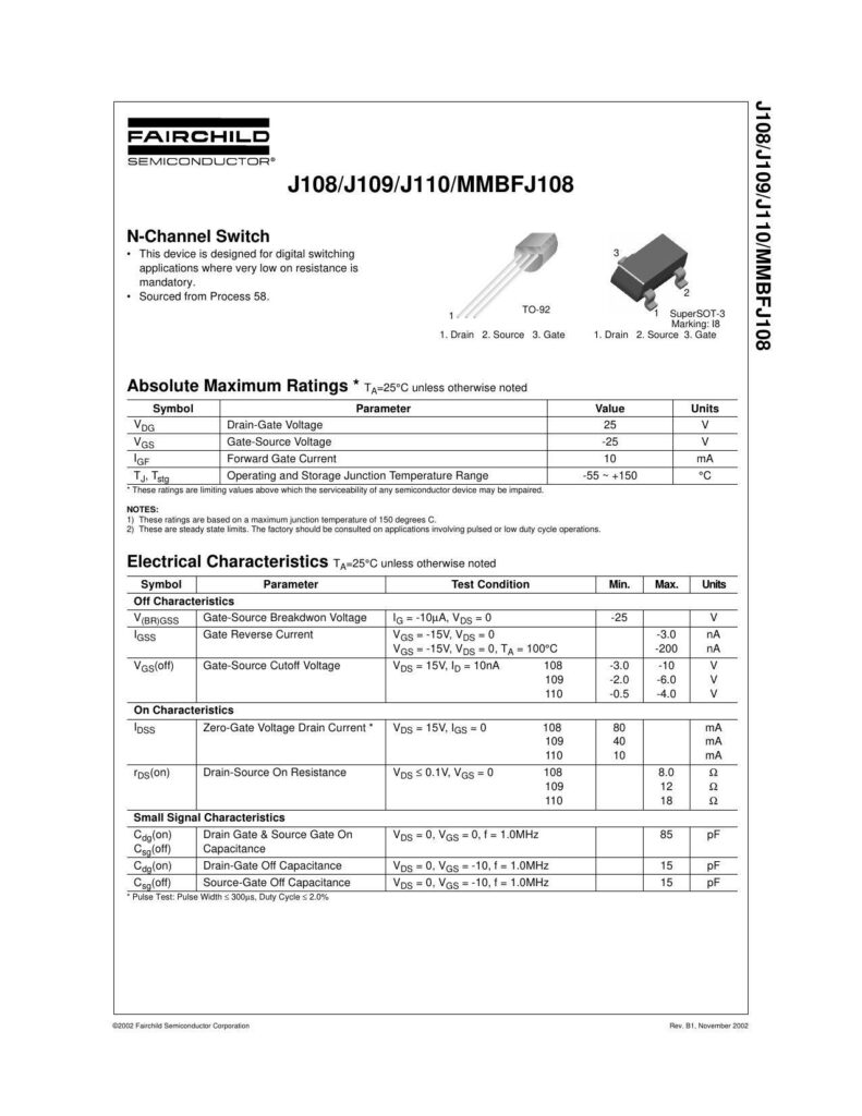
This datasheet describes the J108/J109/J110/MMBFJ108 N-Channel Switch, designed for digital switching applications with low on-resistance.
Absolute Maximum Ratings
The device has a maximum drain-gate voltage of 25V, gate-source voltage of ±25V, and operating junction temperature range of -55°C to 150°C.
Electrical Characteristics
The device has a gate-source breakdown voltage of 25V, gate-source cutoff voltage of 3.0V, and drain-source on-resistance of 6.0 ohms.
Typical Characteristics
The datasheet provides various graphs and charts showing the device’s performance, including drain current vs. drain-source voltage, gate-source voltage vs. drain current, and on-resistance vs. drain current.
The device is available in a TO-92 package with dimensions provided in the datasheet.
Manual:
Chat: Powered By VoiceSphere
Pricing & Distributors: https://www.datasheets360.com/part/detail/j108d26z/-7807895268175797845/