Overview
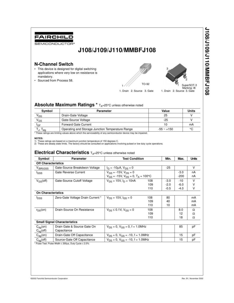
This datasheet describes the J108/J109/J110/MMBFJ108 N-Channel Switch, designed for digital switching applications with low on-resistance.
Key Features
Absolute maximum ratings include a drain-gate voltage of 25V, gate-source voltage of ±25V, and operating junction temperature range of -55°C to 150°C.
Electrical characteristics include a gate-source breakdown voltage of 25V, zero-gate voltage drain current of 10mA, and drain-source on resistance of 6.0Ω.
Thermal characteristics include a total device dissipation of 1.6W and thermal resistance, junction to case, of 125°C/W.
The device is available in a TO-92 package.
Manual:
Chat: Powered By VoiceSphere
Pricing & Distributors: https://www.datasheets360.com/part/detail/j109d74z/3425090441461071618/