Description
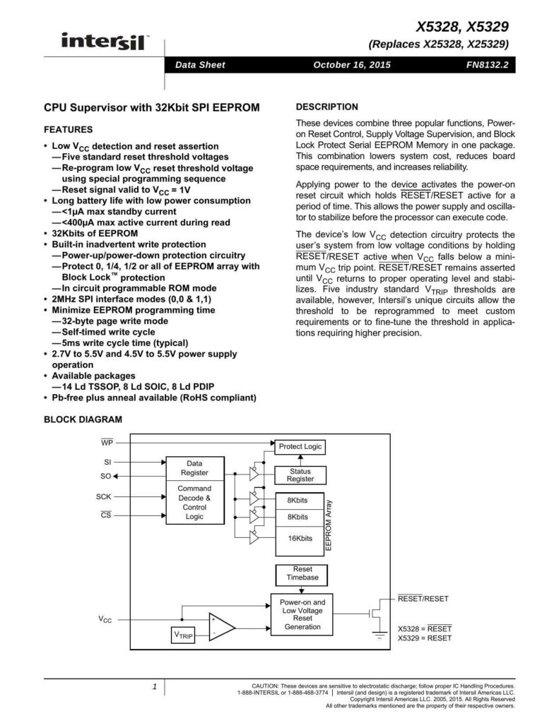
The X5328 and X5329 devices, which supersede the X25328 and X25329 models, integrate a CPU Supervisor with a 32Kbit Serial Peripheral Interface (SPI) EEPROM. Their multifunctional design combines three essential features:
- Power-on Reset Control
- Supply Voltage Supervision
- Block Lock Protection for the Serial EEPROM Memory
This integration aims to reduce overall system costs, minimize required board space, and enhance reliability. Upon power application, the power-on reset circuit is triggered, ensuring the RESET/RESET stays active, allowing time for the power supply and oscillator to stabilize. The device’s low Vcc detection functionality safeguards against low voltage conditions, keeping RESET/RESET active if Vcc dips below a specified minimum threshold.
While five standard voltage threshold (VTRIP) options are available, users have the ability to reprogram these thresholds to suit custom specifications or attain greater precision.
Features
Key features of these devices include:
- Low Vcc detection and reset signal generation, with five predefined reset threshold voltages.
- Users can reprogram the low Vcc reset threshold via a specialized programming sequence.
- RESET signal is maintained as valid until Vcc reaches 1V.
- Battery-efficient operation with <1µA standby current and <400µA active current during reads.
- Built-in write protection to prevent accidental operations on the EEPROM.
- Ability to protect specific portions or the entirety of the EEPROM array using Block Lock protection.
- Enables in-circuit programmability in ROM mode.
- Support for rapid 2MHz SPI with interface modes (0,0 & 1,1) to minimize EEPROM programming times.
- Efficient 32-byte page write mode with approximately 5ms typical write cycle time.
- Supports 2.7V to 5.5V and 4.5V to 5.5V power supply ranges, catering to varying voltage requirements.
- Available in multiple package formats: 14 Ld TSSOP, 8 Ld SOIC, and 8 Ld PDIP.
- Offered in Pb-free plus anneal format, complying with RoHS standards.
Block Diagram Overview
The presented block diagram showcases the internal structure and signal flow of the device. It includes:
- Protection logic
- Status and Data Registers
- Command Decode and Control Logic
- A division of the EEPROM into three segments (two 8Kbit and one 16Kbit section)
- Reset timebase, which includes both power-on and low voltage reset generation circuits
The RESET/RESET output signals are depicted as diverging from the reset generation circuit, with X5328 associated with RESET and X5329 with RESET, for different use case scenarios.
Caution Notice
A cautionary note is provided, emphasizing the device’s sensitivity to electrostatic discharge, necessitating proper Integrated Circuit (IC) handling procedures to avoid potential damage.
Manual:
Chat: Powered By VoiceSphere
Pricing & Distributors: https://www.datasheets360.com/part/detail/x5329s8zt1/-7676803145678236637/

