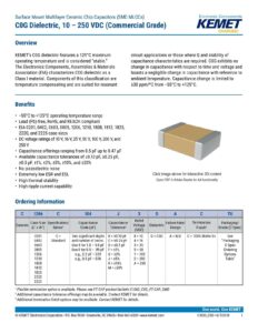
Overview
The 74F04 is a hex inverter integrated circuit (IC) featured in the datasheet from the Philips Semiconductors IC15 Data Handbook. The hex inverter is designed for various applications within the industrial temperature range, which is specified from -40°C to +85°C. Philips Semiconductors provides detailed information about the product’s features, operating conditions, and ordering information, accompanied by illustrations such as pin configurations, logic diagrams, and logic symbols.
Features
One of the key characteristics of the 74F04 hex inverter is its support for an industrial temperature range, making it suitable for environments where standard commercial temperature ranges are inadequate. The datasheet notes an average supply current of 6.9mA for the device and a typical propagation delay of 3.5ns, indicating the IC’s operational speed.
Pin Configuration
The IC is depicted with its 14-pin configuration, including the Vcc pin and the Ground (GND) pin, detailed in their respective positions for easy identification.
Ordering Information
The datasheet provides order codes for the 74F04, distinguishing between commercial and industrial temperature range variants. The commercial range version operates between 0°C to +70°C, and the industrial version between -40°C to +85°C. The order code suffix ‘N’ refers to a 14-pin plastic Dual Inline Package (DIP), while the suffix ‘D’ refers to a 14-pin plastic Small Outline (SO) package. Package drawings are referenced by SOT27-1 for the DIP and SOT108-1 for the SO package.
Input and Output Loading and Fan Out Table
For interface design considerations, the datasheet includes a loading and fan-out table for the inputs and outputs. Each input (Data inputs) can handle a load of 1.0 Unit Loads (U.L.) in both high and low states, while each output (Data output) can drive 50 U.L. in the high state and 33 U.L. in the low state. The loading value is indicated as 20uA in high state or 0.6mA in the low state, with off-state (high impedance) output leakage given as 0mA in the high state or 20mA in the low state.
Logical Functionality
The logical diagram provided shows the internal structure of the hex inverter, indicating how the input signals at pins 1A through 6A are processed to yield inverted outputs at the corresponding pins 1Y through 6Y. A function table is included, further clarifying the IC’s operation: a high input voltage results in a low output voltage and vice versa. For clearer understanding, both the IEC/IEEE symbols and logic symbols are shown, providing an international standard reference for design and application use.
Manual:
Chat: Powered By VoiceSphere
Pricing & Distributors: https://www.datasheets360.com/part/detail/n74f04n/-6608291842486787104/