Overview of Zctel ACT 1 Series FPGAs
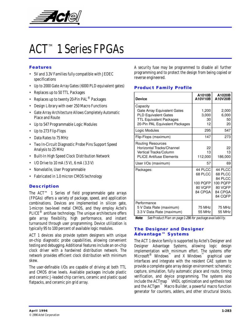
The ACT 1 Series FPGAs from Zctel offer a variety of package, speed, and application combinations. Devices are implemented in 1.0 micron two-level metal CMOS, employing Actel’s PLICE antifuse technology.
Device Features
The ACT 1 devices have a gate array architecture, allowing for completely automatic place and route. They also feature:
- Up to 2000 gate array gates
- Replaces up to 50 TTL packages
- Replaces up to 20 20-pin PAL packages
- Data rates to 75 MHz
- Two in-circuit diagnostic probe pins
- Built-in high-speed clock distribution network
- I/O drive to 10 mA (5V), 6 mA (3.3V)
Design and Programming
The ACT 1 device family is supported by Actel’s Designer and Designer Advantage Systems, allowing for logic design implementation with minimum effort. The systems offer Microsoft Windows graphical user interfaces and integrate with the resident CAE system to provide a complete gate array design environment.
Electrical Characteristics
The ACT 1 arrays have electrical characteristics that remain constant over voltage and temperature fluctuations, making them less prone to delay variation. The total derating factor from typical to worst-case for a standard speed ACT 1 array is only 1.19 to 1, compared to 2 to 1 for a masked gate array.
Package Information
The ACT 1 devices are available in various packages, including plastic and ceramic -leaded chip carriers, ceramic and plastic quad flatpacks, and ceramic pin grid arrays. Refer to the Product Plan on page 1-286 for package availability.
Pin Description
The ACT 1 devices have several pins, including:
- CLK: Clock input for global clock distribution network
- DCLK: Diagnostic clock input for diagnostic probe and device programming
- GND: Ground input
- I/O: Input/output pin with buffered input and output
- MODE: Mode input that controls the use of multifunction pins
- NC: No connection
- PRA and PRB: Probe pins for real-time diagnostic output
- SDI: Serial data input for diagnostic probe and device programming
- Vcc: Supply voltage input
Recommended Operating Conditions
The ACT 1 devices should be operated within the recommended conditions, as specified on page 1-287.
Manual:
Chat: Powered By VoiceSphere
Pricing & Distributors: https://www.datasheets360.com/part/detail/a1010b-2plg68c/-4486926801674823272/