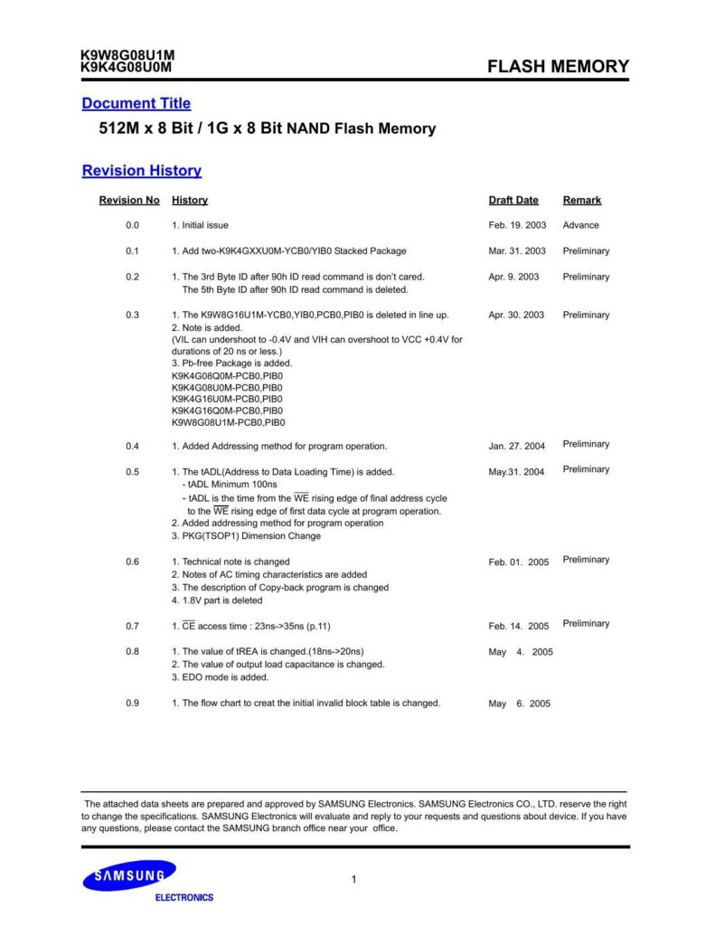
This datasheet describes the K9K4GO8UOM, a 4G bit NAND flash memory device with a spare 128M bit capacity, offered in a 512Mx8bit configuration.
Key Features:
- Voltage supply: 2.7 V~3.6 V
- Organization: Memory Cell Array (512M x 8bit), Data Register (2K x 8bit), Cache Register (2K x 8bit)
- Automatic Program and Erase, Page Program (2K-Byte), Block Erase (128K-Byte)
- Fast Write Cycle Time: Program time 200us (Typ.), Block Erase Time 2ms (Typ.)
- Reliable CMOS Floating-Gate Technology, Endurance: 100K Program/Erase Cycles, Data Retention: 10 Years
Package
The device is available in a 48-pin TSOP1 package, with options for Pb-free packaging and stacked configurations.
Pin Configuration
The pin configuration includes data input/outputs, command latch enable, address latch enable, chip enable, read enable, write enable, write protect, ready/busy output, power-on read enable, power, and ground.
Manual:
Chat: Powered By VoiceSphere
Pricing & Distributors: https://www.datasheets360.com/part/detail/k9w8g08u1m-pcb00/-3057746787801245597/

