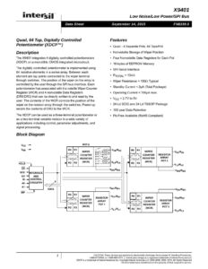
Overview
The U6264B is an 8K x 8 static CMOS RAM featuring advanced memory storage capabilities, with access times as fast as 70 ns. Designed for versatility and efficiency in a range of operating conditions, the U6264B utilizes a common data input/output system and comes with three-state outputs, ensuring compatibility with various system designs.
Power Efficiency and Compatibility
Typical operating supply current is 10 mA at 70 ns, and the standby current is as low as 2 µA at temperatures below 70°C. Moreover, data retention current consumption is under 1 µA at temperatures below 70°C and a voltage of 2 V, providing exceptional power savings during low-power states. For ensuring compatibility with a variety of systems, the U6264B meets TTL/CMOS voltage thresholds and can automatically lower power dissipation in prolonged Read or Write cycles.
Voltage and Environmental Specifications
This SRAM operates at a standard voltage of 5 V and offers an array of operating temperature ranges to suit diverse environmental needs: from 0 to 70°C, -40 to 85°C, and -40 to 125°C. These temperature ranges make the U6264B adaptable for different usage scenarios and requirements.
Quality and Durability
Adhering to the QS 9000 Quality Standard, the U6264B assures reliability. ESD (Electrostatic Discharge) protection is rated at 2000 V according to MIL STD 883C M3015.7, and latch-up immunity is stated at 100 mA, ensuring the integrity of the component under stressful electrical conditions.
Memory Design and Package Options
The memory structure of the U6264B is constructed on a 6-transistor cell base. The NOR gate configuration of the inputs eliminates the need for pull-up/down resistors while contributing to overall low power usage. With two package options available, PDIP28 and SOP28, the U6264B is suitable for a range of board layouts.
Operating Modes and Control
The U6264B offers multiple operating modes such as Read, Standby, Write, and Data Retention. Importantly, during the Data Retention mode, the memory’s contents are preserved even with a minimized power supply of 2 V. The device’s controls include two Chip Enable (E1, E2), one Write Enable (W), and one Output Enable (G), facilitating the necessary command and access structuring for read and write functions.
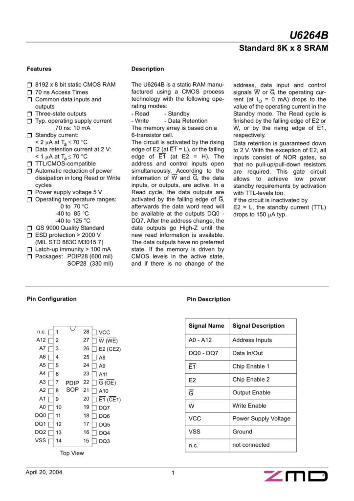
Pin Configuration and Functionality
The pinout includes not only the address inputs (A0-A12) and data input/outputs (DQ0-DQ7) but also the control signals (E1, E2, W, and G), power supply voltage (VCC), and ground (VSS). Additionally, unused pins are denoted as “not connected” (n.c.), aiding in avoiding confusion during the integration process.
Launched on April 20, 2004, the U6264B SRAM stands out for its robust feature set and adaptability to both power-sensitive and demanding environmental conditions, making it a suitable memory storage solution for a wide range of electronic applications.
Manual:
Chat: Powered By VoiceSphere
Pricing & Distributors: https://www.datasheets360.com/part/detail/u6264bs2k07llg1/821461449150541616/