Overview of Microsemi ACT 2 Family FPGAs
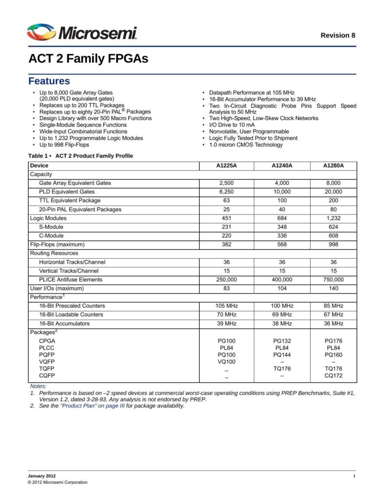
The Microsemi ACT 2 Family FPGA datasheet presents a range of programmable gate arrays optimized for complex digital logic tasks. These FPGAs boast gate capacities ranging up to 8,000 gate array gates, equating to approximately 20,000 PLD (Programmable Logic Device) gates. This gate density enables them to replace a significant amount of traditional TTL (Transistor-Transistor Logic) packages and PAL (Programmable Array Logic) packages, making them a suitable choice for systems requiring high integration and minimizing component count.
Key Features
The ACT 2 FPGAs offer a rich design library, including over 500 macro functions dedicated to streamline development. These functions cover single-module sequence operations, wide-input combinatorial tasks, and a high number of programmable logic modules up to 232. The FPGAs also feature an extensive number of flip-flops (up to 998) to provide robust data storage and synchronization capabilities. High-performance counters and accumulators are explicitly highlighted, citing their operation frequencies of up to 105 MHz for datapath performance and up to 39 MHz for 16-bit accumulators.
Integrated Diagnostic and Performance Tools
For performance analysis and troubleshooting, these FPGAs come equipped with two in-circuit diagnostic probe pins. These pins are instrumental for speed analysis with support up to 50 MHz. Moreover, the ACT 2 roster includes two high-speed, low-skew clock networks ensuring precise timing and synchronization across the FPGA. With I/O pins capable of driving currents up to 10 mA and a nonvolatile, user-programmable logic array, these FGPAs offer reliability and customization for designers.
Programmability and Nonvolatility
All logic configurations are fully tested before shipment to ensure quality and dependability. The use of 1.0 micron CMOS technology contributes to the FPGAs’ robustness and nonvolatility, indicating that programmed logic maintains state without power.
Routing Resources and Antifuse Technology
The FPGAs offer a structured resource grid for signal routing. With up to 36 horizontal and 15 vertical tracks for signal routing per channel, the FGPAs ensure efficient interconnectivity. Their PLICE (programmable low impedance circuit element) antifuse technology provides definitive logic connections that, once programmed, are permanent and low resistance.
Product Family Profile and Performance Notes
A table in the datasheet lists devices within the family, including the A1225A, A1240A, and A1280A, each with varying capacities and resources. Specific resources include the number of logic modules, flip-flops, routing resources, and user I/Os. The performance data are benchmarked against PREP Benchmarks, Suite #1, Version 1.2, which are not endorsed by PREP. Information regarding package availability is deferred to the Product Plan on page III of the datasheet.
The document concludes with revision notes and corporate information, stating its last update as January 2012 by the Microsemi Corporation.
References:
Download: Microsemi ACT 2 Family FPGAs
Chat: Powered By VoiceSphere
Pricing & Distributors: https://www.datasheets360.com/part/detail/a1280a-1pg176b/3354999337295891056/

