Product Overview
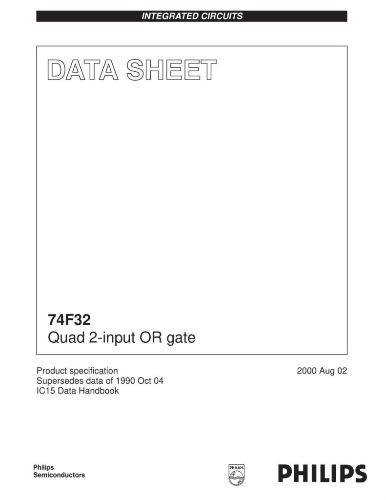
The 74F32 datasheet provides technical specifications for the Quad 2-input OR gate integrated circuits (ICs), which are part of Philips Semiconductors’ product line. This device is intended for use in industrial applications, featuring an extensive temperature range from -40°C to +85°C. The datasheet supersedes the previous data from 1990 and was updated in August 2000.
Key Features
- Industrial Temperature Range: The ICs are rated to operate reliably in conditions ranging from -40°C to +85°C, which makes them suitable for harsh environments.
- Propagation Delay: The typical propagation delay for signals is 4.5ns, indicating swift signal processing.
- Supply Current: The total supply current required for operation is 8.2mA, which specifies the power consumption under normal conditions.
Physical Configuration
The 74F32 IC is laid out in a 14-pin configuration, with the Vcc (positive supply voltage) on pin 14 and ground (GND) on pin 7. Input pins are represented as Dna and Dnb, and the corresponding output for each OR gate is referred to as Qn.
Pin Configuration
The datasheet includes a diagram labeled SF00038 that provides a clear visualization of the IC’s pin layout, outlining each input, output, Vcc, and GND positioning.
Product Variants
Available in both commercial and industrial ranges, the 74F32 IC comes in two order codes for each range:
- N74F32N and 174F32N: For the commercial range operating from 0°C to +70°C.
- N74F32D and 174F32D: For the industrial range operating from -40°C to +85°C.
Package drawings referenced, SOT27-1 and SOT108-1, correspond to the 14-pin plastic dual in-line package (DIP) and the 14-pin plastic small outline (SO) package, respectively.
Input/Output Characteristics
The datasheet presents an Input and Output Loading and Fan Out Table, wherein logical IOs like Dna and Dnb (data inputs) and Qn (data output) are specified along with their respective load values, given in FAST (Fairchild Advanced Schottky TTL) unit loads.
Logical Operative Diagram and Function Table
A logic diagram labeled SF0039 is included, showing the internal structure of the OR gates as well as an IEC/IEEE symbol diagram (SF0040 and SF0041) representing the logical function of the IC. Additionally, the function table lists the output state (Qn) in relation to the input states (Dna, Dnb).
References:
Chat: Powered By VoiceSphere
Pricing & Distributors: https://www.datasheets360.com/part/detail/n74f32n/-7893010572653209968/

